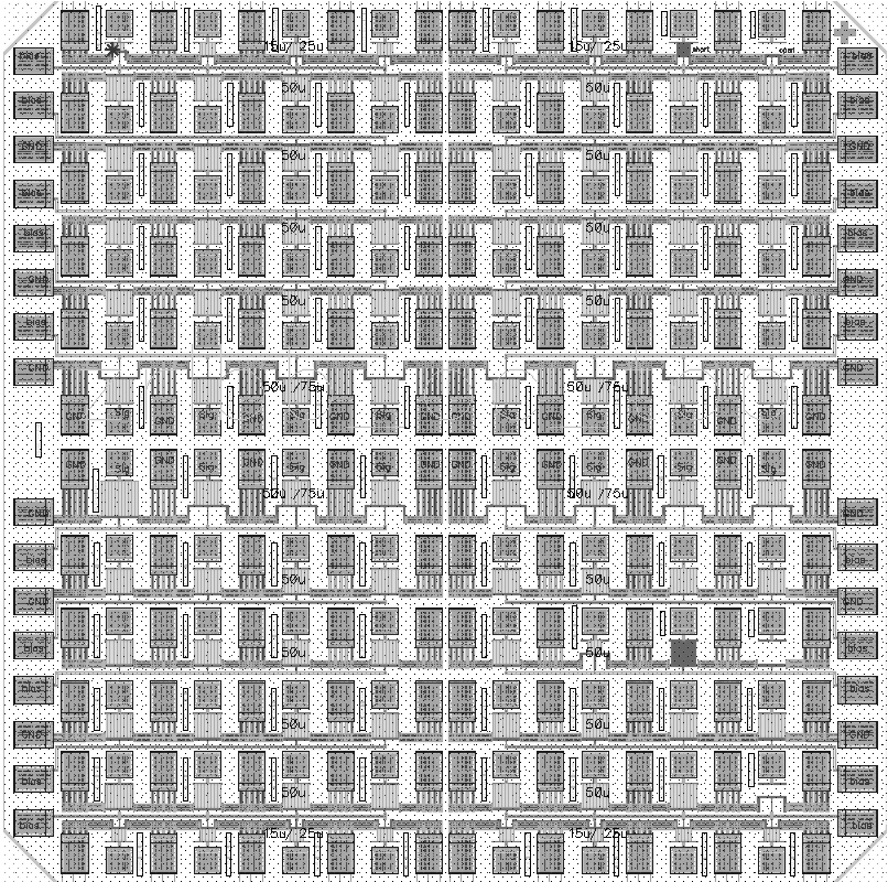
Optical detector in standard CMOS SOI
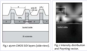
Standard Complementary Metal Oxide Semiconductor (CMOS) Silicon on Insulator (SOI) technologies are not very well suited to absorb electromagnetic radiation because silicon has an absorption length of several hundred micrometers at the interesting wavelengths and the absorbing layers are in the range of several ten nanometers. Therefore, special techniques are required to enhance the absorption in the active silicon layer.
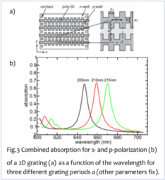
While some groups utilize Germanium, which is also available in some standard SOI technologies, we use frequency-selective resonant geometries in polysilicon to maximize absorption of electromagnetic radiation. Simulations of the two-dimensional resonant gratings show absorption rates of close to seventy percent in a layer of some ten nanometer thickness. Compared to six percent in the same layer without resonant structures this is significant. In theory and from simulations the resonant structure is expected to increase the absorption rates for a specific optical frequency by over a factor of ten by using two-dimensional resonant gratings.
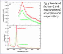
Measurements have shown that resonances and absorption peaks exist but are slightly shifted and not as high as expected. Inspections with a microscope revealed that metal fill layers (used in the semiconductor process to safeguard planar surfaces and prevent out-of-focus conditions during mask processing) cover the active regions of the detectors. A silicide layer used for the same reason additionally covered the active area and prevented radiation to reach the absorbing layer. Cross-verifications with simulations indicated that such coverage can cause the effects.
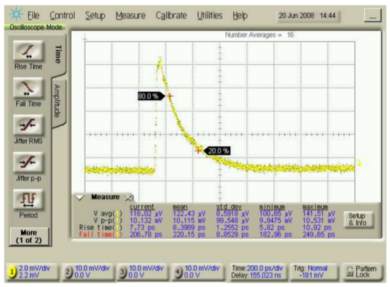
The measured minimal signal rise time was 8.5 picoseconds for resonant detectors with small detector active areas. This turned out to be about three times faster than the rise time observed with one-dimensional gratings. In case of no grating no signal was detected (measured) at all because of a huge absorption length compared to a tiny absorption layer. The signal rise time increased to approximately 40ps for the largest detectors on the experiment.
Finally, proper resonant structures cause frequency-selective absorption peaks in tiny layers from electromagnetic resonances and fast signal rise times. Resonant structures and active areas of detectors needs to be uncovered to support coincidence of predicted and measured resonances and maximize absolute absorption. Signal rise times depend on the detector size so that small detector areas and maximum absorption rates appear most promising. Resonances depend on the incidence angle of the incoming signal having a direct correspondence to frequency and wavelength so that peaks of absorption occur for distinct frequencies at distinct angles of incidence in one resonant structure.
Publications
[1] N. Moll, T. Morf, M. Fertig, T. Stoeferle, B. Trauter, R. Mahrt, J. Weiss, T. Pflueger, "Polarization-Independent Photo-Detectors with Enhanced Responsivity in a Standard SOI CMOS Process", IBM Research Report on Electrical Engineering, May 18th 2009.
[2] N. Moll, T. Morf, M. Fertig, T. Stoferle, B. Trauter, R.F. Mahrt, J. Weiss, T. Pfluger, K.-H. Brenner, "Polarization-Independent Photodetectors With Enhanced Responsivity in a Standard Silicon-on-Insulator Complementary Metal–Oxide–Semiconductor Process", IEEE Journal of Lightwave Technology Vol. 27, Issue 21, pp. 4892-4896 (2009).
Patents
[1] M. Fertig, N. Moll, T. Morf, T. Pflueger, Photo detector and integrated circuit, US Patent Application Publication 2013/0093035 A1, Apr 18th 2013[2] M. Fertig, N. Moll, T. Morf, T. Pflueger, Computer implemented design of device for electro-optical modulation of light incident upon device, US Patent Application Publication 2012/0246608 A1, Sep 27th 2012
[3] M. Fertig, T. Morf, N. Moll, M. Kreissig, K.-H. Brenner, M. Auer, Device for detecting electromagnetic radiation comprising a diffusion junction and resonant grating in a single layer, US Patent Application Publication 2012/0206723 A1, Aug 16th 2012
[4] M. Fertig, T. Pflueger, T. Morf, N. Moll, Using 3d integrated diffractive gratings in solar cells, US Patent Application Publication 2010/0101638 A1, Apr 29th 2010
[5] M. Fertig, T. Morf, J. Weiss, T. Pflueger, N. Moll, Photo detector device, US Patent Application Publication 2009/0179225 A1, Jul 16th 2009
[6] M. Fertig, N. Moll, T. Morf, T. Pflueger, J. Weiss, Photo detector, US Patent Application Publication 2009/0140362 A1, Jun 04th 2009
Contact
Prof. Dr. Matthias FertigAlfred-Wachtel Straße 8
78462 Konstanz
Tel: +49 (0)7531 206 269
Email: mfertig(at)htwg-konstanz.de
Project-Team
- IBM ZRL, Rüschlikon, CH
- Dpt. of Optoelectronics,
Inst. of Computer Eng.,
Univ. of Heidelberg, GE - IBM R&D, Böblingen, GE