Introduction to the Digital ASIC Design Flow
| Name of the course | Online | Lecture | Exercises | Lab |
|---|---|---|---|---|
| Digital ASIC Design Flow Lab | ✓ | ✗ | ✗ | ✓ |
Context
Preliminary courses/knowledge:
Recommended Preliminary courses:
- Basic knowledge in Unix/Linux and shell script
- Introduction to Digital Circuit Design [w3]
- Microprocessor Architecture [w3]
Follow-on courses:
Details
The course offers a low-level entry into the world of digital ASIC design for prospective engineering managers or ASIC design engineers. The laboratories include all steps from logic entry to layout data and the major critical engineering corners and project milestones are explained.
The course aims for engineering managers to define work packages, create time plans, interpret engineering outputs and track development cycles. Candidates with a sound background in digital engineering get introduced to the technical complexity of digital ASIC engineering. All participants are trained on a contemporary up-to-date design environment as utilized in industry.
The course is founded on the Cadence Design Environment using the Cadence Acacdemic License. This guarantees a full-functional set of tools at industrial standard, excellent documentation and support as well as regular updates so that the course offers an up-to-date design environment at all times.
The course is offered barrier-free in a virtual classroom. Presence is mandatory to complete the course successfully. Physical presence at the campus is possible but not required.
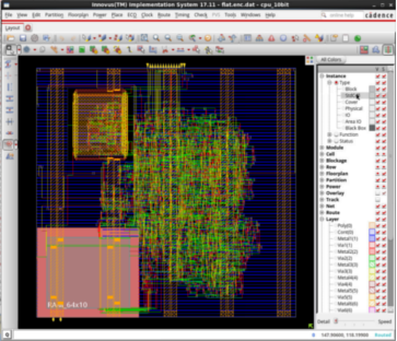
Participants work on different ready-to-run digital ASIC design flows and on ready-to-use designs during the entire course. It is not necessary to develop new designs or to setup and configure a design flow from scratch. Participants investigate the flow of design data along the chain of tools and how the results develop along the process.
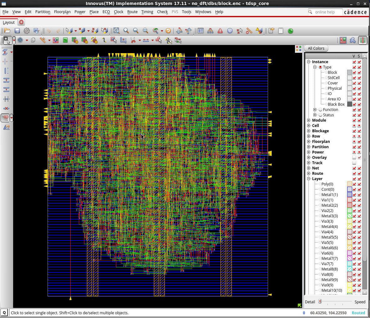
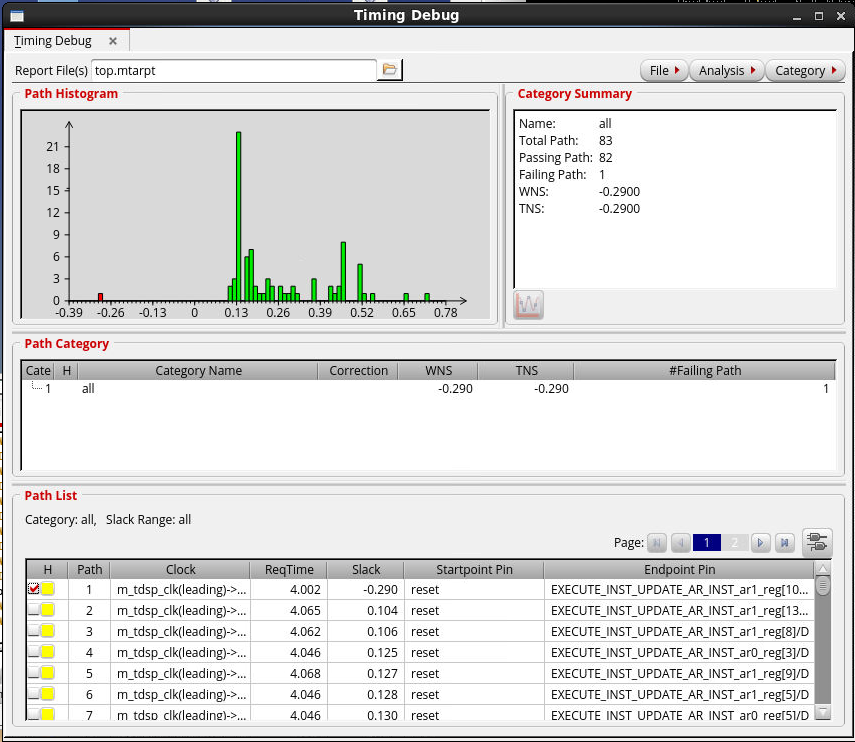
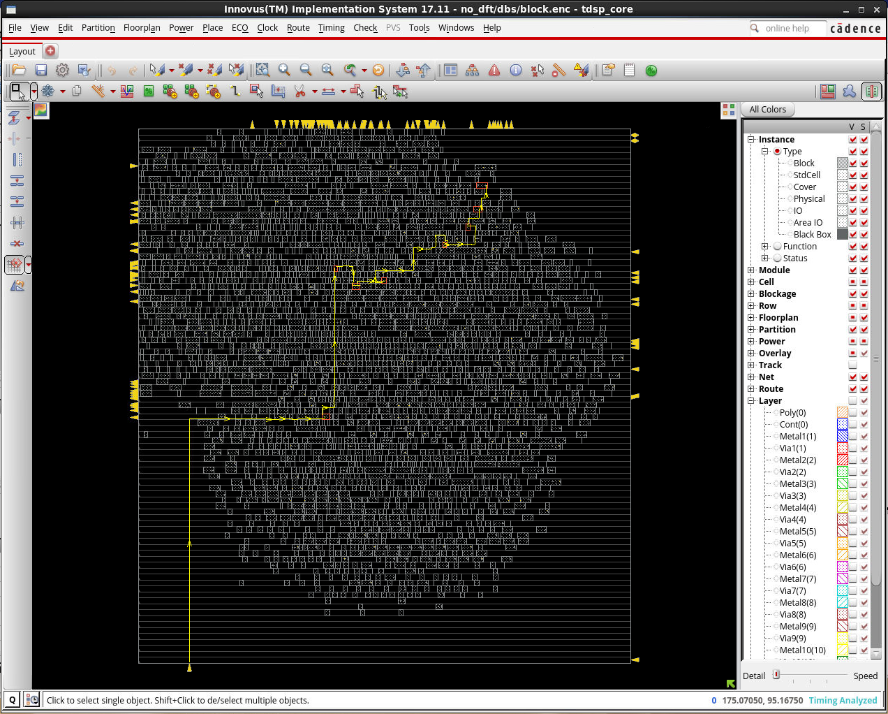
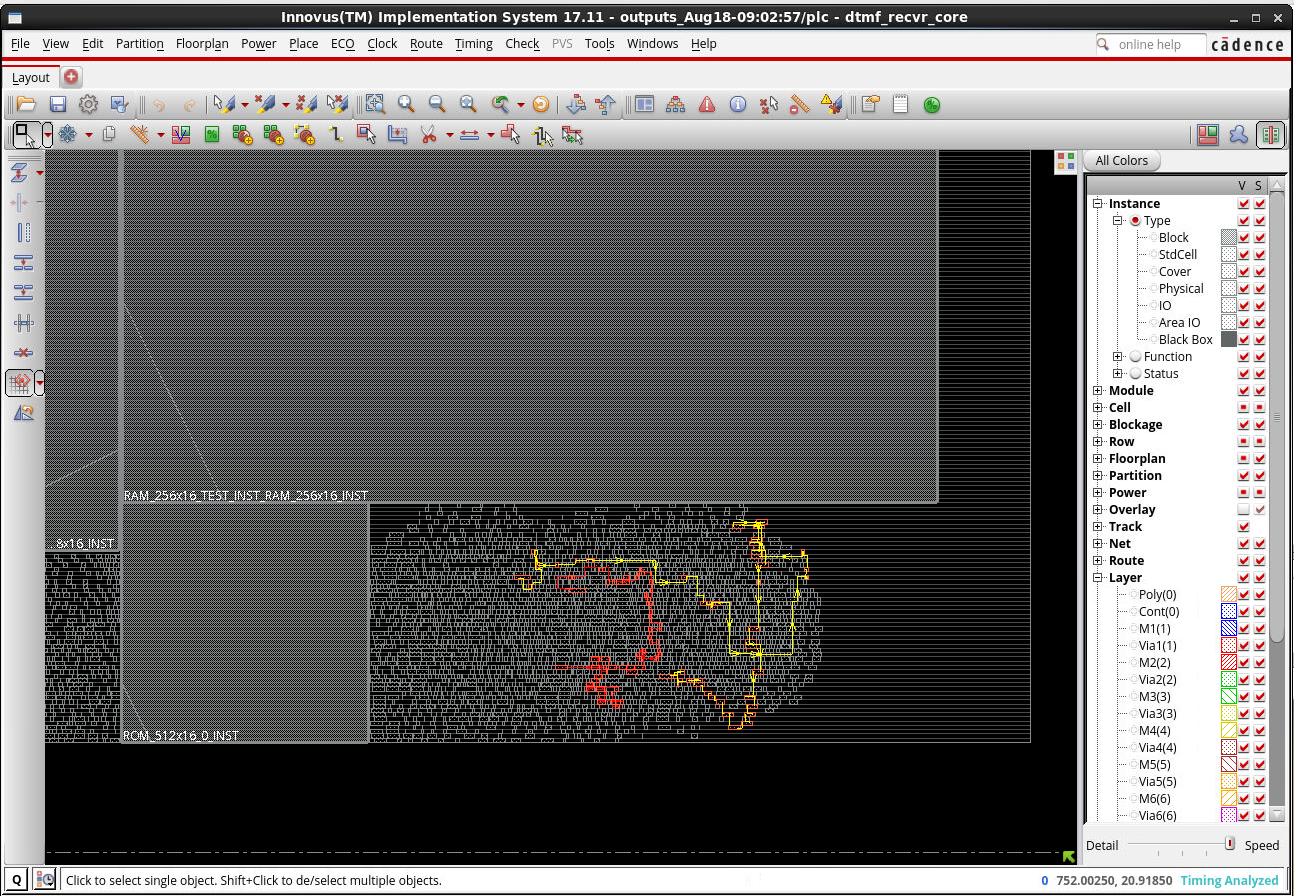
The course offers lab exercises on the general design flow as well as on specific design aspects, e.g. Engineering Change Orders, Low Power, 3D-Integration. The output of a sample exercise can be found here.
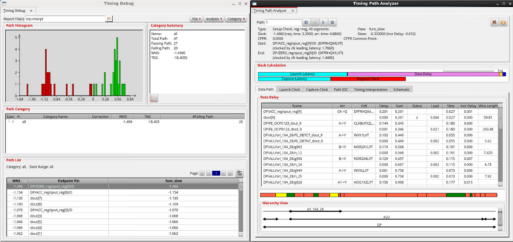
Lab Exercises
| Num | Description | BSc | MSc |
|---|---|---|---|
| 1 | Introduction to the Digital Design Flow | ✓ | |
| 2 | Introduction to the Digital ECO Flow | ✓ | |
| 3 | RTL to GDSII implementation of a tiny Digital Signal Processor (DSP) | ✓ | (✓) |
| 4 | Static Timing Analysis of a Dual-Tone Multi-Frequency Reveiver (DMTF) | ✓ | |
| 5 | Synthesis of a Dual-Tone Multi-Frequency Reveiver (DMTF) | ✓ | |
| 6 | Power Profiling of a 10-bit CPU design at RTL level | ✓ | |
| 7 | Low-power implementation of a SiFive P670 RISC-V CPU core | ✓ | |
| 8 | 3D Integration of a two-die RISC-V design | ✓ |
Participants work on the labs remotely on a university server using individual VNC sessions. Attendance from a computer room at the university is possible but a personal computer is recommended to connect to the server and work independent from opening hours.
Literature
[1] CMOS VLSI Design, 4th edition by Weste Neil Harris David, 2010, ISBN-13 978-0321547743[2] Application Specific Integrated Circuits, Michael Smith, 1997, ISBN-13 978-0201500226, [w3] or [w3]
[3] Cadence documentation and training material
