RAPID - A Digital Design Package for VHDL
Logic entry at register transfer level (RTL) is a time consuming task and synthesis results depend on the expressions utilized in the HDL code.
While some expressions yield proper synthesis results in terms of circuit size and speed, others do not despite their logical equivalence.
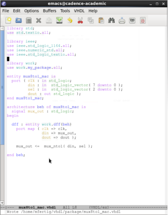
In order to avoid iterations in logic entry apart from verification issues, obtain good synthesis results and support a maintainable and service- able code structure, the Rapid Digital Design Package provides a set of common functions and building blocks to be used as function calls in the VHDL. The functions have been worked through the entire design flow. The package contains multiplexers, en- and decoders, parity gene- rators as well as gate functions for boolean vectors.
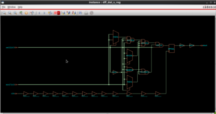
Synthesis creates the netlist of the 8to1 mux as shown in the right figure. The cone is traced down to a latch which is attached to the output of the mux. The clock tree is built from buffer instances as shown in the bottom of the circuit.
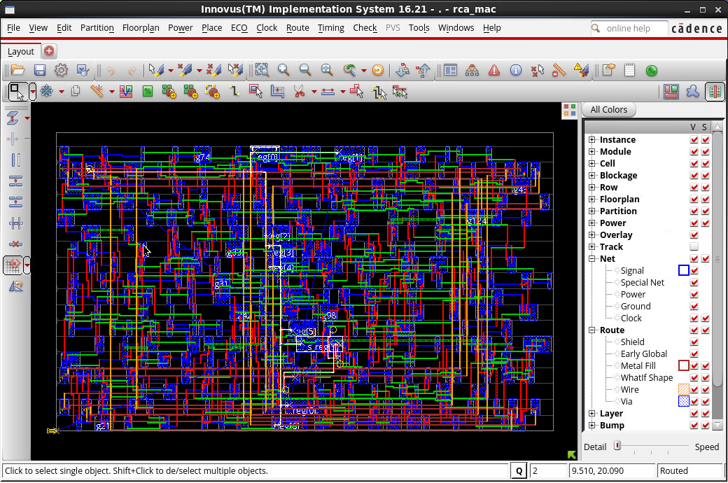
The layout step creates the semiconductor and metal layers as shown in the left figure. A simple mux8to1 example has been selected to verify the scripts used in the design flow.
Ripple-carry, carry-lookahead and carry-save adders of configurable width are available.
Example: 4-port ripple-carry-adder w/ overflow indication with RAPID
All adders in the RDDP provide configurable width. An n-port adder can be built in a single line or, if the intermediate results shall be visible in simulation, an adder-tree is built.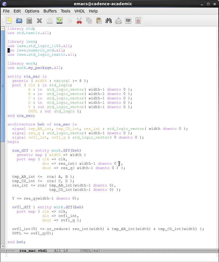
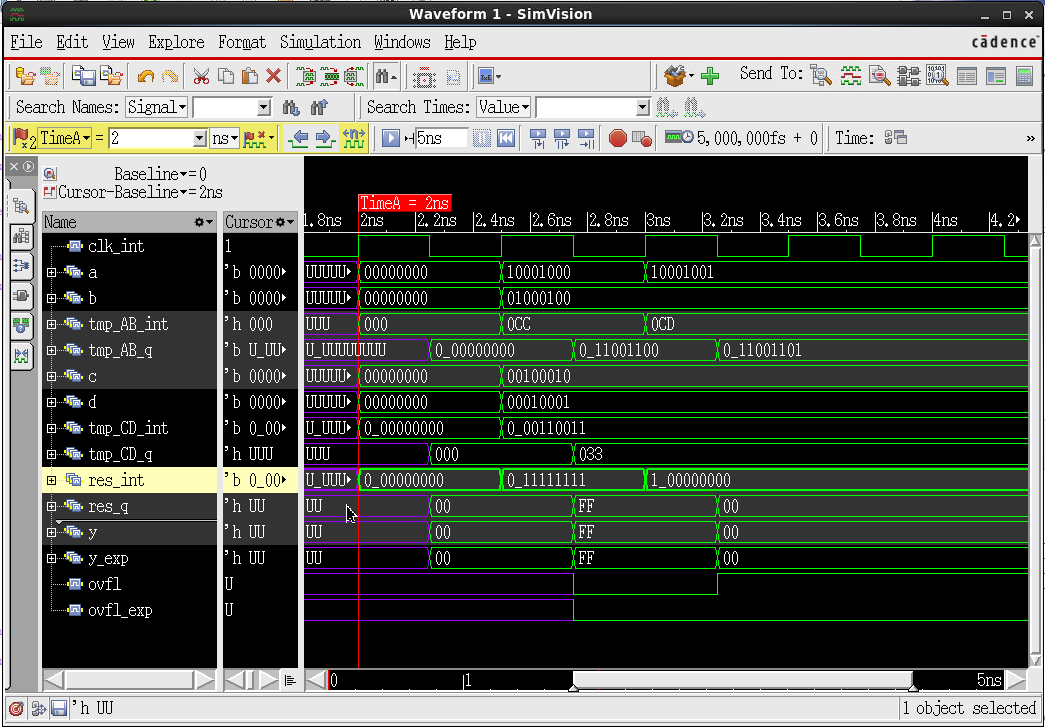
Testcases are simulated in a testbench to verify the basic functionality of the design.
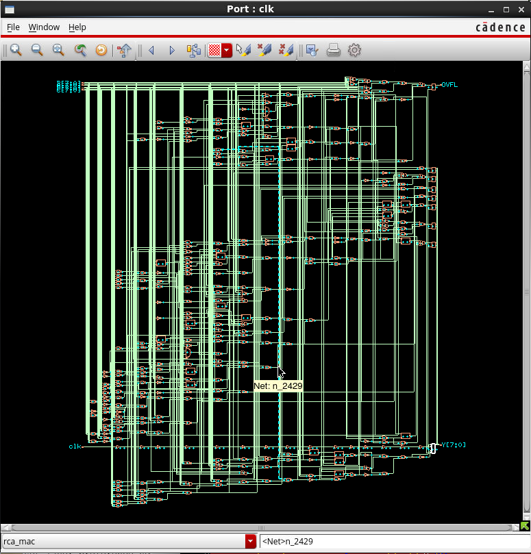
In a synthesis run, the netlist is derived from the VHDL or Verilog model.
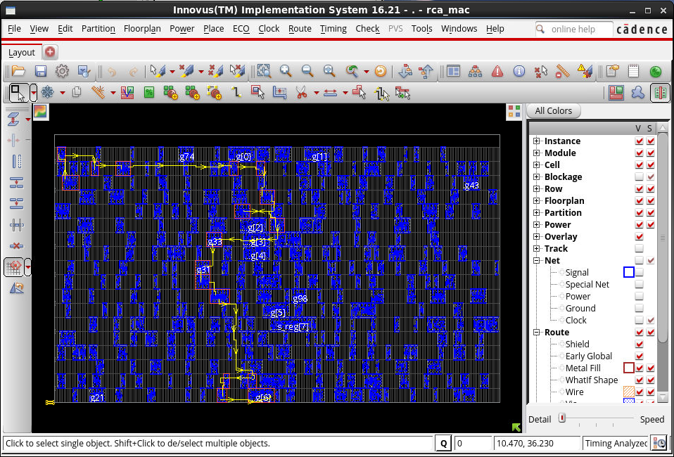
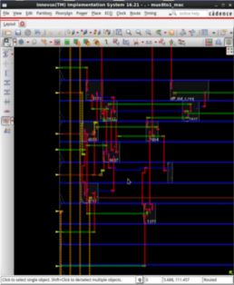
The floorplan defines the available area for the place and route tools. The clock-tree and power/gnd connections as well as the interconnects between the gates in the netlist are formed in silicon using the technology library, e.g. a 45nm CMOS SOI technology as shown here.
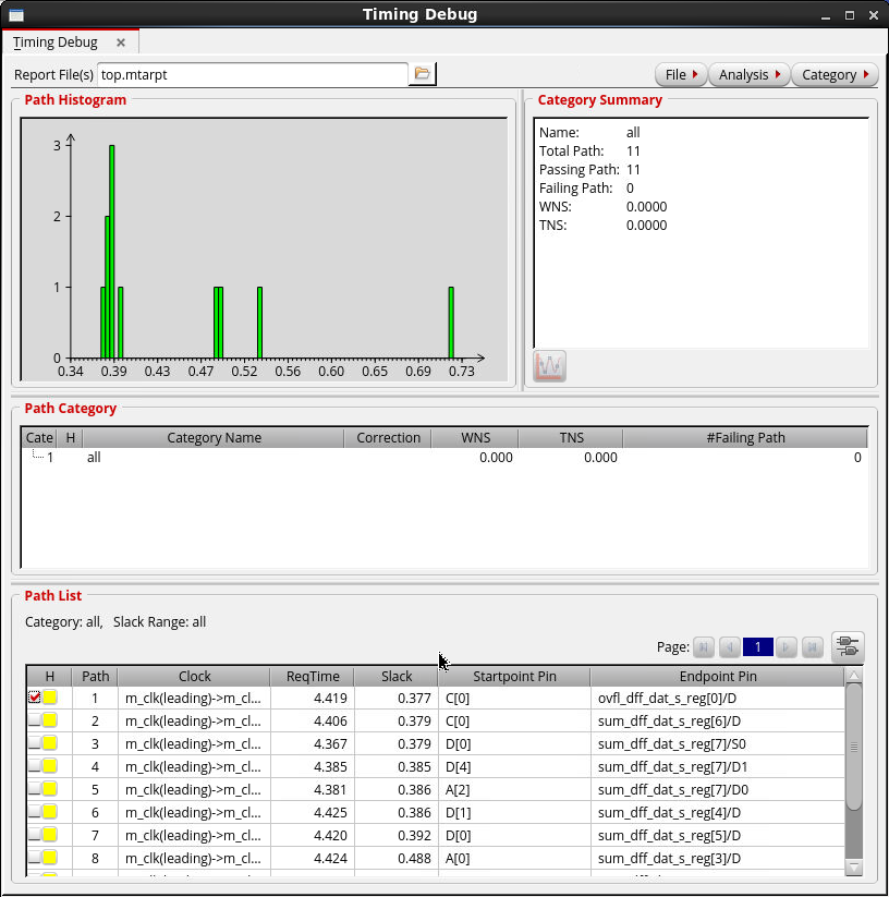
After place and route, a timing is performed on the results to verify if the design operates at the intended clock cycle time(s). At this step, physical and logical checks (DRC/LVS) are performed to secure proper functionality of the circuit. Noise budgets are derived from RLC-extractions to analyse the design for noise sensitive regions.